|
|
3D-IC Work |
Thermal and stress modeling was part of the large amount of 3D-IC work done at RPI and Albany Nanotech, as part of the Interconnect Focus Center. That work continues at Process Evolution. |
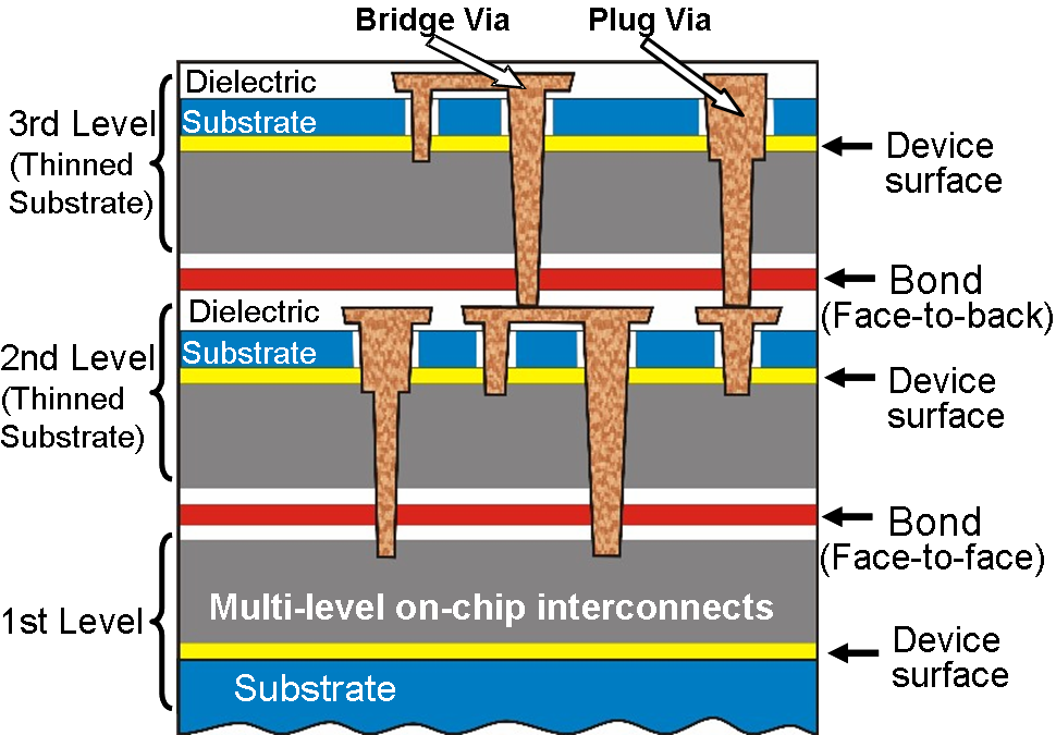
We have studied thermally induced stresses in 3D-ICs, with an emphasis on the vias
that interconnect the circuits on two wafers; i.e., the 'interwafer vias' which might wee be
"TSVs" (through silicon vias).
We have focused our efforts on wafers glued together using BCB, and interconnected using copper
interwafer vias. See the figure below. In addition to several other papers on this and
related studies, see "Three-Dimensional Integration in Microelectronics: Motivation, Processing
and Thermomechanical Modeling", T. S. Cale, J.-Q. Lu and R. J. Gutmann, Chem. Eng. Comm. 195, 847-888 (2008).
See for example: J.-Q. Lu et al., 2002 IITC, IEEE, 2002, pp. 78-80
The goal is to determine if thermal expansion can be a reliability issue, due to
the differing thermal expansion coefficients in the bonded wafers. We used
Comsol Multiphysics
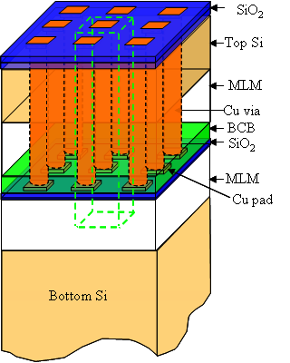
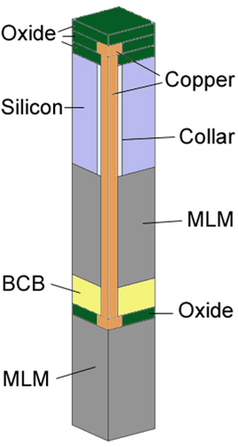
for this phase of our thermomechanical modeling. The figure on the left above
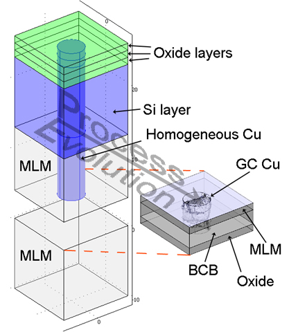
shows an idealized field of vias through muultiple materials.The image on the
right above shows a view of one quarter of a via and bounding materials, as used
in the simulations.
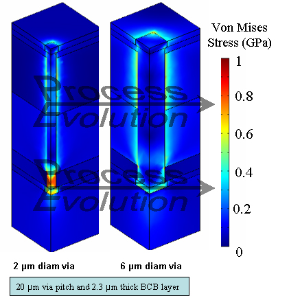
Results using models that treat all of the materials in the via structure as traditional continua show that there is reason to be concerned about thermally induced stresses in BCB-bonded wafers. This is basically because BCB has a much larger coefficient of thermal expansion (CTE) than Cu. As shown in the figures below, the highest stresses induced in the copper interwafer vias are where they pass through the BCB layer.
|
|
|
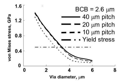
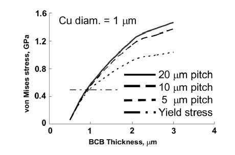
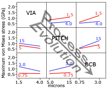
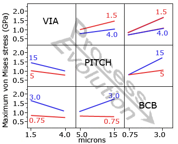
(left) Computed von Mises stress distributions, due to a temperature change of 100 K, on
cross-sections of two via structures, for two different via diameters, for the
specified pitch and BCB thickness.
(right) (top)Computed von Mises stress vs. via diameter for the listed BCB thickness and via pitches
(right) (bottom) Computed von Mises stress vs. BCB thickness for the listed via diameter and via pitches
See for example: J. Zhang et al., IEEE Trans. Sem. Man. 19(4), 437-448 (2006)
Note that for a fixed BCB thickness and pitch, the smaller via diameter has the larger von Mises stresses in the copper as it passes through the BCB. Depending upon the values of such design parameters, there may be problems with stability, as the stresses can be beyond reasonable estimates of yield strength.
To improve our model for 3D-IC via structures, we introduced grain structures, as it is easy to show that polycrystalline models of copper can result in very different induced stresses than models that treat copper as homogeneous.
PLENTE is used to generate and represent the grains in polycrystalline models of 3D-IC vias. As the region of most interest is the via as it passes through the BCB layer, we focus our attention there. In order to reduce the computational burden of representing the entire via as grains, we studied how much of the via needed to be represented as grains. That is, we computed the stresses induced in the region of the BCB layer, using granular representations of different lengths of the via. We found that We needed to represent about the via a grains for about 1 grain size outside of the BCB layer.
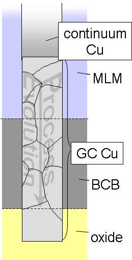
After developing this hybrid of traditional continuum and grain-continuum approaches, which we call a 'hybrid grain-continuum' or HGC repressentation of the structure, we compared computed maximum induced von Mises stresses against those from tradtional continuum (TC) models of via structures.
We compare the results of HGC and TC models by using PLENTE and COMSOL Multiphysics as a virtual testbed to generate DoE (Design of Experiments) models for the same region of design parameter space. In this study, two values (levels) were chosen for (each) via diameter, via pitch and BCB thickness, and a temperature change of 100 K was considered.
For the same design parameters, the trends are the same
(qualitatively the same results for TC and HGC models), but the maximum
von Mises stresses induced by the temperature change are higher when using
HGC models than when using TC models.
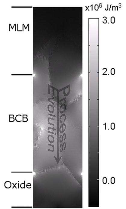
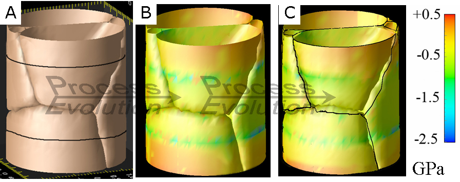
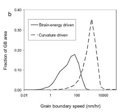
Given a distribution of stress and strains throughout the domain of an HGC representation, the motion of the grain boundaries can be computed. Some results are summarized by the following figures. An image of strain energy density on a cross section of a 3D-IC via is shown on the left. On the top right are images that show how the HGC approach was used to predict evolution. The graph on the bottom right shows that strain energy driven evolution is slower than curvature driven evolution.
|
|
|

PE Home
About PE
Contact PE
EVOLVE AMR
EVOLVE MM
EVOLVE 3D
EVOLVE
3D-ICs
PLENTE