
|
PLENTE
|
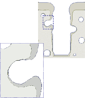
Coarsening of Cu line
|
PLENTE is the Parallel Environment for Nanoscale
Topography Evolution.
PLENTE was used in several significant studies, as noted below. While the
paragraphs below are valid, PLENTE has been replaced by
EVOLVE MM, because of the latter's ability to
extract consistent interfaces. Nevertheless, this url provides considerable
information about the kinds of studies we can do.
At its heart, PLENTE is a generalized 3D multiple material
geometry and topography tracking software. That means that it can be used
to track not just 1 phase, but many distinct, interacting phases, which
makes it ideal for tracking grain structures as they form and evolve. The
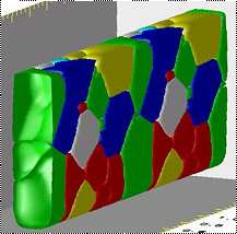
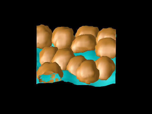
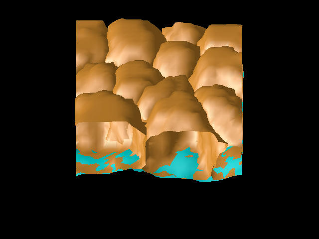
image and clip to the right show grains in an IC interconnect line being
processed: The still shows an initial set of grains, while the clip shows
the evolution of the grains due to curvature - over the period of many
hours (lab time).
PLENTE uses a finite element solver to track level sets as they
evolve. Because it uses not one, but an arbitrary number of level sets,
PLENTE can represent many interacting, but distinct, phases and the
boundaries which develop and evolve between them. This ability to
track phase boundaries has allowed us to use it in a "grain-continuum"
context, that enables us to quickly simulate grain and grain boundary
motion. PLENTE has been developed for use in a cluster environment,
although a couple of processors are enough for small problems.
We have used PLENTE to study several processes and phenomena, including:
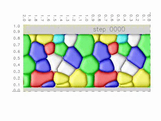
Please look at the sample screen shots and movies of PLENTE simulation results below. Notice
that some of the examples combine PLENTE with
EVOLVE.
Such combined studies can now be done with
EVOLVE MM
(which replaces PLENTE) and
EVOLVE 3D
(which is a 3D/3D extension of the "3D/2D" EVOLVE).
Stress-induced grain boundary evolution
Stress-induced grain boundary evolution
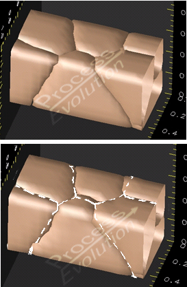
3D grain boundary motion driven by strain energy differences. The stress field for a set of
grains with anisotropic mechanical properties, embedded in silicon dioxide, was calculated
using
Comsol Multiphysics.
Individual grains were assigned
orientations based upon which interior surface each one nucleated on (predominantly <111>
but with one anomalous <100> grain as well) and single-crystal Cu properties were mapped
onto the orientation. A temperature drop of 100K from a stress-free state was imposed and the
stresses due to thermal mismatch were computed. Then, grain boundaries were moved in response to
differences in strain energy across them. White dotted lines in the "after" picture show positions
of original grain boundaries. (The encasing dielectric is not shown.)
The emphasis of this project is on the representation and evolution of 3D
grain structures, and interactions with Comsol. We used a simple elasticity model to compute
thermally induced strain energy densities for demonstration, but this can be generalized.
ELD
ElectrolessDeposition on a Rough Surface
 Various stages and view angles of a simulation of electroless deposition (ELD) onto a
substrate of 5 nm RMS roughness. The last frame is of the final grain structure seen by
looking through a transparent substrate. See the movie of this copper deposition on a
rough surface.
Various stages and view angles of a simulation of electroless deposition (ELD) onto a
substrate of 5 nm RMS roughness. The last frame is of the final grain structure seen by
looking through a transparent substrate. See the movie of this copper deposition on a
rough surface.
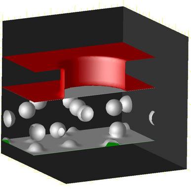
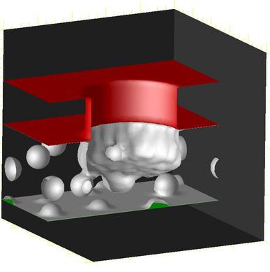
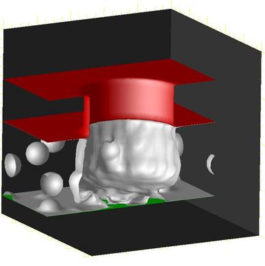
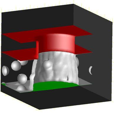
Electroless Deposition into a Trench
Various stages and view angles of a simulation of electroless deposition (ELD) into a
1.3 aspect ratio trench. The last frame is of the final grain structure seen by looking
through a transparent substrate. See the movie of this copper deposition into a
trench.
See a similar copper deposition into a
set of repeating infinite trenches
using a periodic boundary condition.
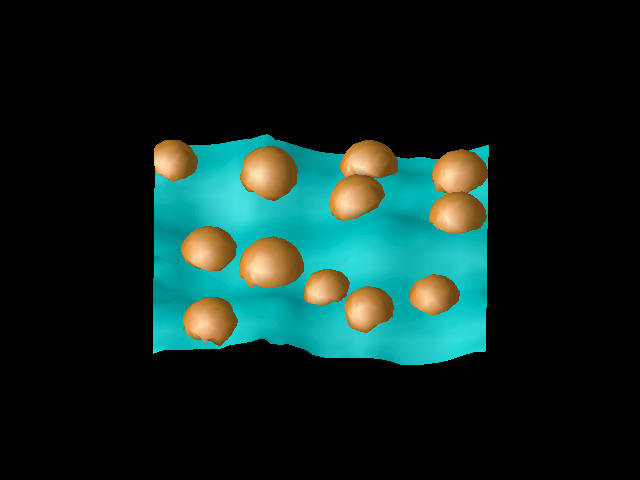
Grain Formation
Grain Formation during Vapor Deposition
Limited area deposition from the vapor phase onto islands nucleated onto a substrate.
The substrate is nonreactive (except at nucleation sites, which saturate quickly). The
sticking on the substrate in each case is zero. The sticking factors on the deposit
are 1.0 (top), 0.5 (middle), and 0 or isotropic (bottom). The cross sections on the
right indicate that film density increases with decreasing sticking factor.
Annealing
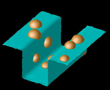
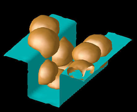
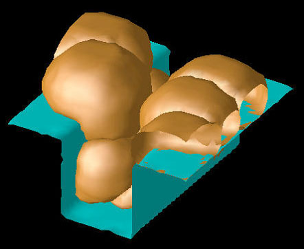
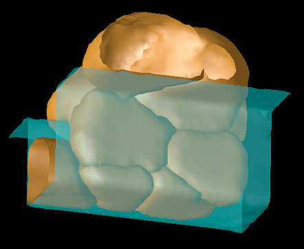
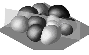
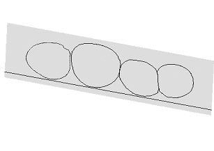
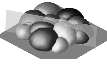
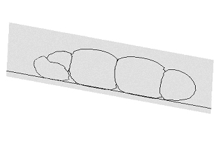
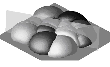
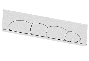
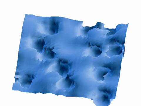
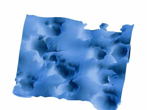
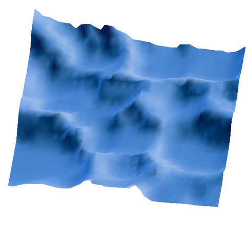
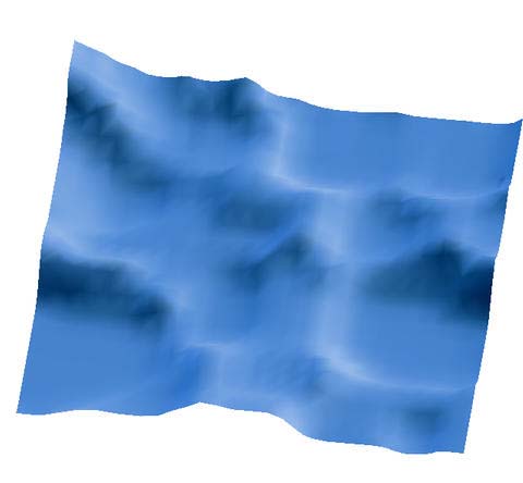
Grain Coarsening During Annealing
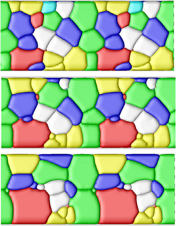
Curvature driven (Gibbs-Thompson) grain coarsening simulation using physical
properties representative of copper, at 360 K. The initial structure is formed
using an electroless deposition simulation. An angle view of the initial structure
(part of a line) is shown on the left. On the right are three "snapshots" at
selected times during the simulation, initial (top), 500 min. (middle)
and 1000 min (bottom). An animation of this simulation can be found
here.
Grain Size Distributions
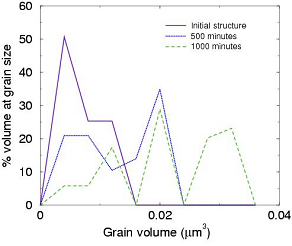
Grain size distributions as extracted from structures (as pictured above) at
selected times during the coarsening simulation; time = 0, 500 min, and 100 min.
Other important characteristics can be extracted from the simulations.
Porous Dielectrics; Etching and Deposition
As a generalized geometry and topography tracking software, PLENTE can
be used to track etch processes as well. Below we have two simulations
that combine both PLENTE and EVOLVE
to simulate etching.
We show both ion milling and reactive ion etching, which uses a
chemical kinetics based model inside EVOLVE, performed through a
patterned mask into a porous substrate.
Ion Milling of a Porous Dielectric
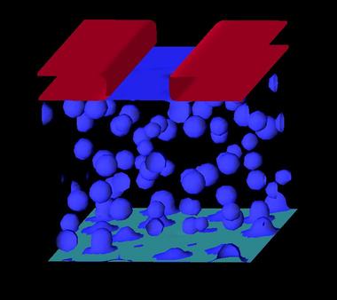
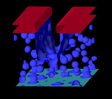
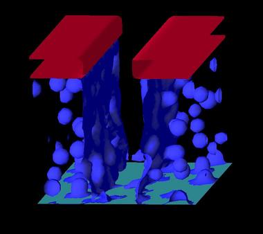
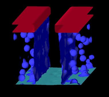
(above) Several still frames of an aspect ratio 2.5 trench being
etched into a substrate with 30% porosity.
Full movie.
Reactive Ion Etching of a Porous Dielectric
(above) Cut-away view of several frames of an aspect ratio 1.0 via
being etching into a substrate with 10% porosity.
Full movie.
(above) Simulation of PVD sealing of a porous dielectric in a trench. This is
cross section of a 3D deposition simulation, after a 3D etch simulation
similar to the above simulations.
Barrier Comformality
Damascene Structure Initial Structure and with Deposited Barrier
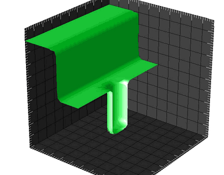
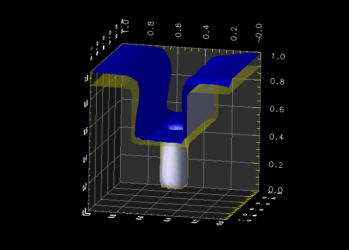
Ta PVD simulation into a dual Damascene structure. (left) Initial dual damascene
structure and (right) barrier shown with initial structure.
Barrier Thickness as a Function of Position
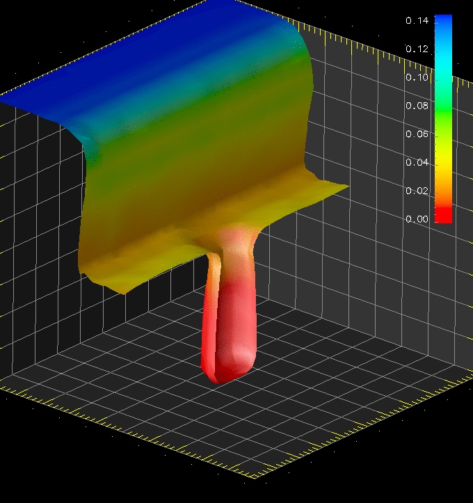
Color map of deposited film thickness. Areas less that 10 nm are shown in red;
the films is 140 nm thick on the flats.
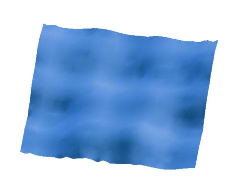
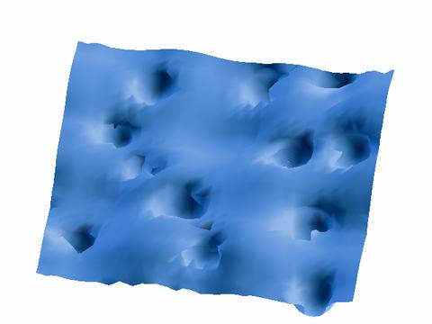
Corrosion
PLENTE can be used for more than just microelectronic and microstructural applications.
Below are several frames of a corrosion simulation on an
initially slightly rough surface.
Corrosion is isotropic after pitting through the intial protective coating on the surface.
Snapshots of Corrosion After Pinhole Formation in a Protective Coating
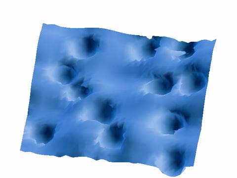
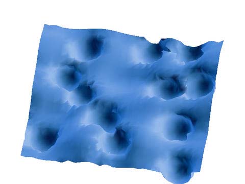

Long time behavior, after all of the initial surface has been eaten away.

PE Home
About PE
Contact PE
EVOLVE AMR
EVOLVE MM
EVOLVE 3D
EVOLVE
3D-ICs
PLENTE